Electronics Design and Production
Assignment
- Use KiCad to design a development board to interact and communicate with an embedded micro controller.
- Make and test the development board you designed.
More information can be found on the 
Installing KiCad
To get started, I downloaded the following tools:
Installing Fab Electronics Library in KiCad
On the GitLab repo, there are installation instructions:
- Clone or download the Fab Electronics Library and rename it to fab.
- Store it in a safe place such as ~/kicad/libraries or C:/kicad/libraries.
- Run KiCad or open a KiCad .pro file.
- Go to "Preferences / Manage Symbol Libraries" and add fab.kicad_sym as a symbol library.
- Go to "Preferences / Manage Footprint Libraries" and add fab.pretty as a footprint library.
We were instructed to watch a YouTube series from Fab Lab Reykjavík, which is linked 
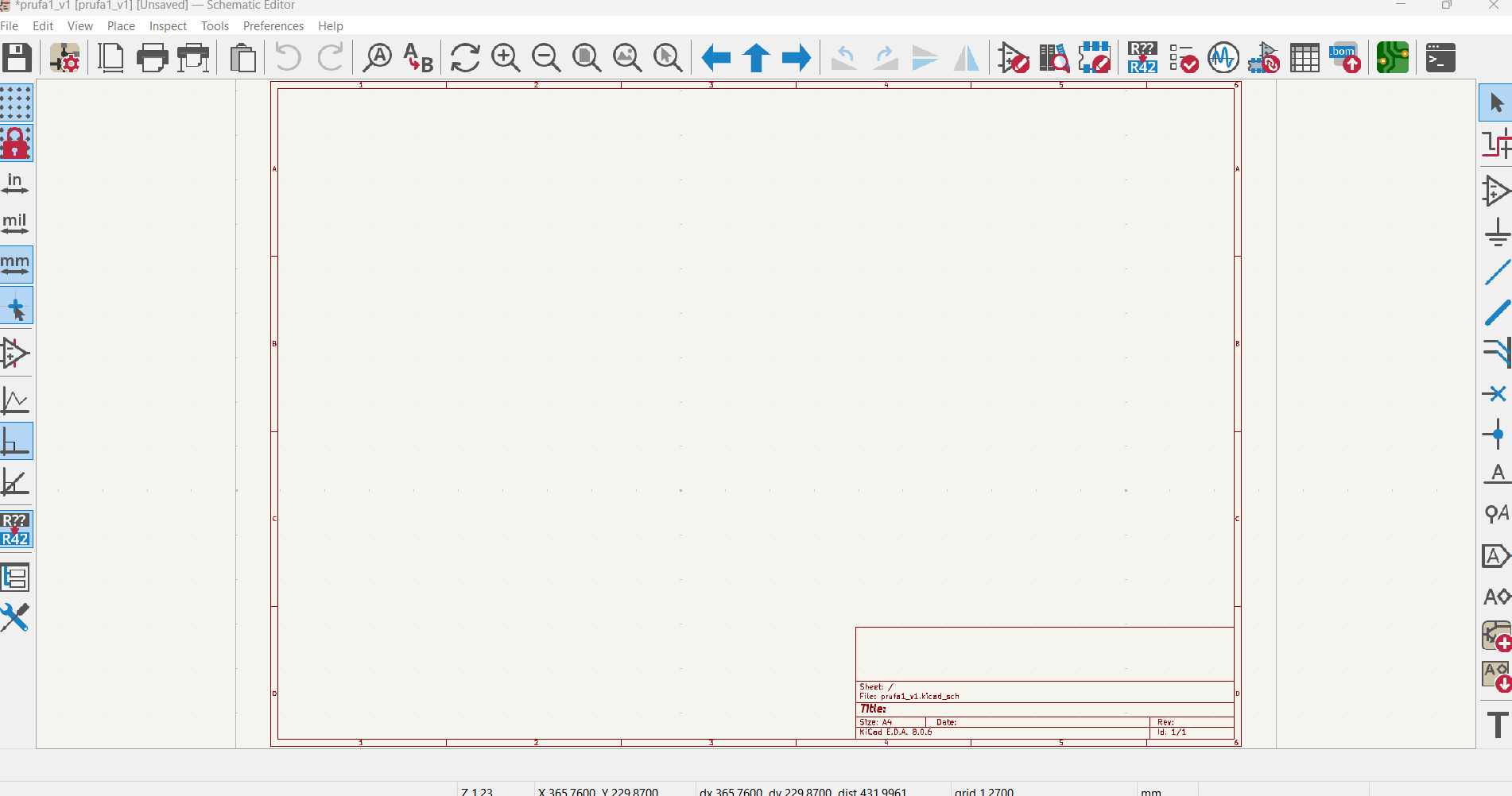
After installing these tools, I started by creating a project folder. Then, I opened KiCad, made a project, and opened the Schematic Editor.
The Schematic Editor

I began by adding the following components:
- ATtiny 412
- Switch_Tactile_Omron
- C_1206
- L_1206
- Conn_PinHeader_1x03
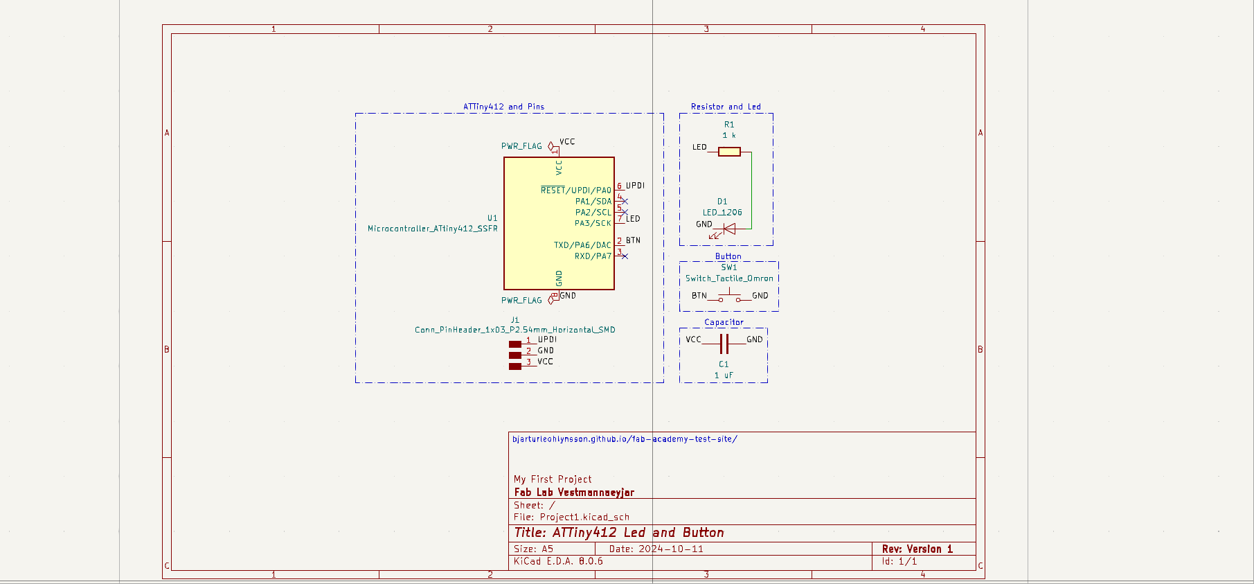
After adding the components, I connected all of them together and labeled everything. Then, I changed the paper to A5 and labeled it. Finally, I had something that looked like this:

The PCB Editor
(Needs images)
Next, I opened the PCB Editor by pressing this button on the toolbar in the schematic editor

Next i synced my schematic to the PCB editor by pressing F8
Then, I arranged the components and started connecting them together following the labels I had made in the Schematic Editor. So I had this:
To finish, I placed a square outline to tell the computer how large the board was supposed to be. Then, I had this which I could use to make the board.
Lastly, as a secondary task, I opened the 3D viewer and assigned all the components 3D models so I could use that as a reference to model a case or something similar in FreeCAD.
Exporting and Inkscape
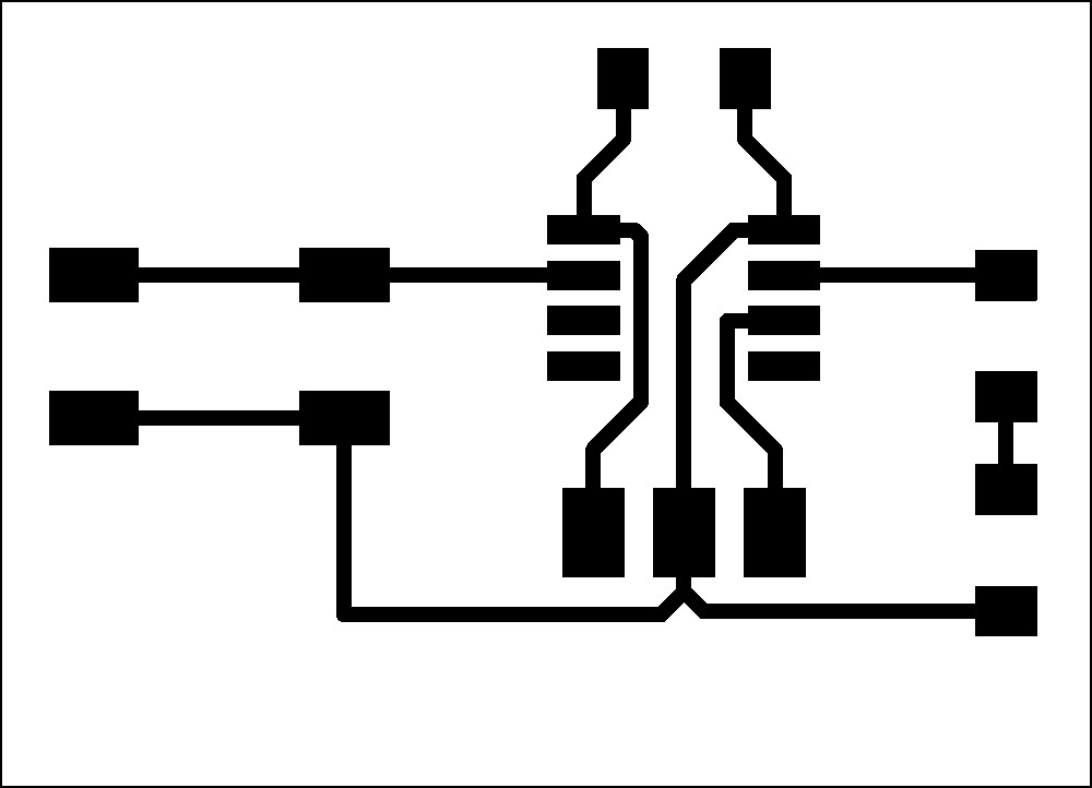
Next, I had to export my KiCad board so I could mill it using the circuit mill. I went into export and selected F_CU and exported it as an SVG. Then I did it again but now I only selected Edge_Cuts. Now I had two SVG files that looked like this:


The second image does include a line around the edge but it is only visible in light mode. Next, I opened up Inkscape and inverted the colors so white was black and black was white. Now I could export it again and I was ready to mill!